The repo contains the KiCad files for manufacturing the printed circuit board and front panel for a 4-channel Eurorack active mixer, based on the one Hagiwo assembled by hand here. This project is a simpler precursor to building a Eurorack module with a Daisy Seed, in order to hone my skills and go one-time through the PCB manufacture process.
For this design I am aiming to:
- use through-hole components only
- mount the pots and jacks directly onto the PCB
- as opposed to just securing them to the panel and wiring each individually to the board (as in the original Hagiwo design)
- place all component on a single board (no stacking)
- this will limit the number of inputs to 4 (instead of Higawo's 5)
- also design the module front panel as a PCB and have it manufactured at the same time
- 4 x 10K potentiometers Alpha 9mm (inputs)
- 1 x 100K potentiometer Alpha 9mm (output)
- 6 x Thonkiconn 3.5mm jack sockets
- 1 x TL072 dual op-amp (integrated circuit in PDIP package)
- 1 x 2x5 Pin Shrouded Header (Eurorack power connector)
- 5 x 100K resistors
- 1 x 22K resistor
- 1 x 4.7K resistor
- 1 x 1K resistor
- 2 x 4.7uF electrolytic capacitors (block out high-frequency AC noise or ripple that might be present on the DC power supply line.)
- Design the schematic
- Simulate the circuit (TODO)
- Design Eurorack board templates
- Assign footprints and place components
- Route traces
- Design the front panel
- Produce gerber files
- Do a test laser cut (or paper print)
- Send to manufacturer
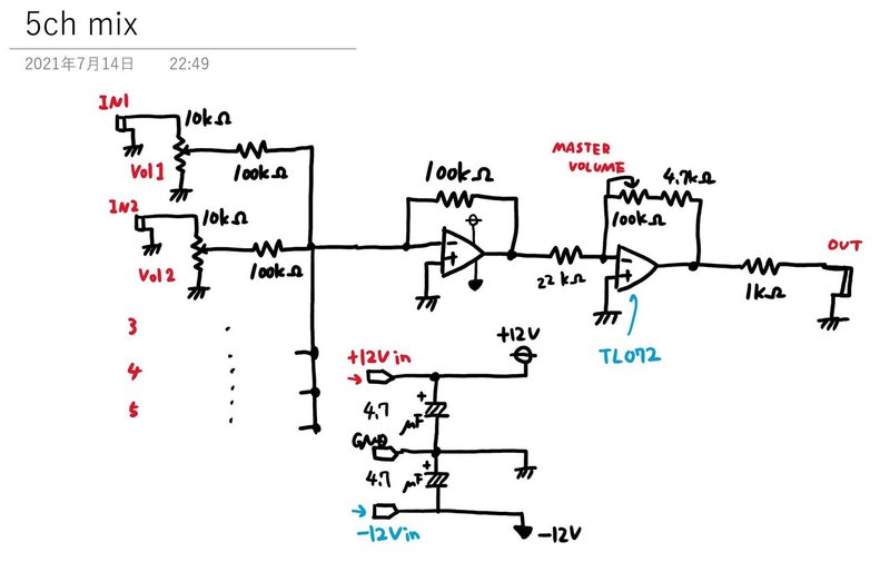
I am following Hagiwo's hand draw schematic, as referenced here:
The Doepfer schematic detailed on this page is also useful for comparison, but includes some extra details and differences.
To understand the schematic, I found it helped to describe it briefly in terms of signal flow:
- We attentuate the incoming signal from each jack input using a potentiometer
- The signals are then mixed together and fed to the input of an operational amplifier
- The op amp attentuates the signal by a fixed level (to compensate for the volume increase of the combined inputs)
- A potentiometer across second op amp acts as a master volume, attentuating the mixed signals
- The attentuated output goes to the jack output
I'm using AudioJack2_SwitchT as the jack symbol on the schematic. It has only tip and sleeve, where:
- the tip is the "hot" pin which should carry the audio signal to the potentiometer input
- the sleeve goes to ground
Designing the mixer helped me get to grips with how to supply power to a module from a Eurorack power supply.
Key points:
-
Power comes in via a 10-pin shrouded power header
- Shrouded means that the cable can only be inserted one way
- The symbol for this can be found in the eurocad library under the name
EURO_PWR_2x5 - From the 10 pins it is standard practice to short together:
- the two +12v rails
- the two -12v rails
- the six ground pins
-
The +-12V rails are used to power our TL072 dual op-amp chip
- When placing the TL072 dual op-amp schematic symbol, we must click three times
- twice for each individual op amp
- once for the power part of schematic
- When placing the TL072 dual op-amp schematic symbol, we must click three times
-
2 x 4.7uF electrolytic capacitors are used between the +12V and -12V rails and ground
- their purpose is to smooth out unexpected small fluctuations in voltage
-
some useful principles of voltage control and power in Eurorack are also covered here
The aim here is to check that the signals meet Eurorack output levels
Key points:
- we will use Spice simulation
- advice is to replace potentiometers with fixed value resistors and vary the values between simulation passes
- So check for a given input that we get an expected output
- But what inputs to use?
- the schematic needs to be reworked to be suitable for a PSPICE simulation (It isn't as simple as "hit run, get a waveform.")
- AC Sweep is probably the analysis method to use
I found it important to first design superimposed templates for both the front panel and main PCB. This is because the holes in the front panel template will be derived directly from the centre hole positions of the jacks and pots on the main board.
My starting point was this repo of Euroack KiCad project templates. Unfortunately, there was no 6HP template, so I used the opportunity to design my own.
The width of Eurorack modules is measured in HP (Horizontal Pitch), where one unit of HP is 5.08mm wide (0.2 of a an inch). Fortunately our KiCad grid already has a setting for this.
I started by defining three templates, using the original Doepfer specifications. This online converter was also useful.
- this is the exact 6HP width and normal height i.e. 30.48mm x 128.5mm
- it is helpful to keep everything on a HP grid
- i used a dotted outline and placed it on the User Drawings layer, as it won't be used for manufacture
- this is 0.24mm narrower either side and the same height i.e. 30.00mm x 128.50mm
- it also includes two oval screw mounting holes (enough for modules < 12HP):
- the horizontal centre of which should be 1HP in from the edge
- the vertical centre of which should be 3mm from the edge
- diameter should be 3.2mm
- width of the oval should be 5.2mm
- I placed it on the Edge Cuts layer, as it represents the milled board outline
- this is 0.5mm narrower still either side than the front panel and not as tall i.e. 29.00m x 106mm
- the reduction in height is necessary so that the board passes the mounting rails
- I placed it on the Edge Cuts layer, as it represents the milled board outline
In KiCad, rectangles are specified using x and y start and end points. Here are points for all the elements mentioned above:
| Item | X Start | X End | Y Start | Y End |
|---|---|---|---|---|
| Front Panel Template | 0 | 30.48 | 0 | 128.5 | Front Panel | 0.24 | 30.24 | 0 | 128.5 |
| Mounting Hole 1 | 5.08 - 2.6 | 5.08 + 2.6 | 3 - 1.6 | 3 + 1.6 |
| Mounting Hole 2 | 30 - 5.08 - 2.6 | 30 - 5.08 + 2.6 | 128.5 - 3 - 1.6 | 128.5 - 3 + 1.6 |
| Main Board | 0.74 | 29.74 | 11.25 | 117.25 |
Note on mounting holes: - my mounting holes are oval and 5.2mm wide and 3.2mm tall - for hole 1, we go from the top left (0, 0) and then - move one HP to the right on the X axis, then add/subract half of the oval width - move one 3mm down on the Y axis (Doepfer standard), then add/subract half of the oval height - from hole 2, we go from the bottom right (30, 128.5) and then - move one HP to the left on the X axis, then add/subract half of the oval width - move one 3mm up on the Y axis (Doepfer standard), then add/subract half of the oval height
Once all three templates were complete, I grouped them all together to ensure they are not accidentally moved out of position relative to one another. It is also possible to snap different elements within the design to grid points, to aid relative placement of components.
Before the components can be laid out on the PCB, a footprint for each must be given in the schematic. Below are the footprints I used for some key components, some of of which are taken from the eurocad library
| Component Name | Footprint Name |
|---|---|
| 3.5mm Jack Sockets | eurocad:PJ301M-12_T_S |
| Potentiometers | eurocad:Alpha9mmPot |
| TL072 Dual Op Amp | Package_DIP:DIP-8_W7.62mm |
| Shrouded Power Header | Connector_IDC:IDC-Header_2x05_P2.54mm_Vertical |
There are tools available purely for doing front panel design, such as Front Panel Designer and Synth Panels Designer. These could help to define the ideal component placement in future, but this time round I just placed by hand using the main board height as the core constraint.
Key points:
- Placement was done within the bounds of the main board template
- The height of the board (106mm) limits the design to five rows of jack potentiometer pairs in total
- If the components were not mounted on the board directly
- an extra row could be squeezed in
- or the existing rows could be better spaced
- I followed this simple design constraint:
- For input rows: Jacks on the left, pots on the right
- For output row: Jack on the right, pot on the left
- The jack and potentiometer pairs were placed at equal vertical distance from one another
- The KiCad measurement tool came in handy to check this
- The remaining components were placed in the spaces between the pairs, and the power connector at the bottom
Key points:
- We use only two layers (front and back)
- The PCB component holes are 'vias' which allow the traces to be routed between the two layers
- I followed a simple 'ground plane' convention to decide which traces to put on which of the layers, which states that all connections that go to ground should be on one side of the board (the back) and all other connections on the other side (the front)
- I used thicker traces of 0.5mm for the power traces leading from the power header to the capacitors and op amp. This I had seen recommended in other designs.
- For all other traces I used the default thickness of 0.25mm
Designing the front panel was a relatively simple matter of:
- Creating mounting holes whose centre points match those of the circles on the jack and pot footprints
- Moving the panel template, plus mounting holes to one side (still on the grid)
- Adding text, row markers and logos as drawings to the silkscreen layer
- Mirroring the design at the end, so that the silk screening is visible when we flip the panel over to place it on top of the pot/jack shafts
Key points:
- To make the mounting holes, I oriented the grid so that the centre of the existing components was directly on a grid boundary
- The diamater of the mounting holes was as follows
- Alpha 9mm pots: 7mm
- Thonkiconn jacks: 6mm
- To make the holes, use the "Add a footprint" icon and select searching for
MountingHole- Unlike plain circles, this makes sure they actually get included in the Gerber drill files
- Note: Mounting hole footprints are measured in radius, not diameter, so I used 3.5mm and 3mm variants
- For cooler visual effects, it is also possible to draw on the solder mask layer or experiment with surface finishes (e.g. ENIG vs HASL)
Once all the above has been done, we can use the File -> Save a Copy option in the PCB Editor to make PCB Only and Panel Only versions of our project and then delete the elements we don't need. We need to do this so the files can be read properly as separate projects by the manufacturing house.
Key points:
- Go to
File Menu -> Plotto start the export process for each board- Click
Generate Drill Files- this should create a set of .drl files - Also Click
Generate Map File- this helps for laser cutting/paper printing a template (see below) - Then click
Plot- this should create a .gbr file for each KiCad layer
- Click
- Both the drill and Gerber files should be checked in KiCad's inbuilt Gerber viewer
- the .gbrjob file contains all the layers in one file, so is easier to quickly check (though the individual files are what will actually be sent)
- don't forget to check the .drl (drill) files as well as these are not included in the .gbrjob file
As we have a laser cutter in-house, I was able to produce a test cut of the pcb and panel to help check my component dimensions. A paper print would also do the job, but with a laser cut you can also seat the components and check stability etc.
I overcomplicated it and need a better workflow for next time. Ideally I would be able to export a single .svg file containing just Edge Cuts and the drill file holes combined.
Some tips:
-
We can produce drill map files as well as drill files, as these can be open directly in the pcb editor
- Note that they don't appear in the .gbrjob file
-
If we don't want to use drill files,
Edge CutsandF_MaskorB_Masklayers would do -
It would be best to stay in the pcb editor, as we can export .svg's directly from it
- Unfortunately it produces one .svg per layer, which we then have to combine manually!
Plot on All Layersfunction may helpDrill markssection may help, but I couldn't get the marks to appear
- Unfortunately it produces one .svg per layer, which we then have to combine manually!
-
Probably avoid working in the Gerber viewer directly. This is because:
- we have the .gbrjob file, but it doesn't contain drill file layers
- creating drill map files that can be open and copied directly into our main PCB Editor file is better
- we can't export .svg's directly from the Gerber viewer, so we end up having to export back the PCB Viewer anyway!
- one last-resort option would be to install on the laser cutter PC and use 'Print' option for Gerber viewer, but I don't like it!
- we have the .gbrjob file, but it doesn't contain drill file layers
-
component heights should be such that they all poke through the front panel at the same height (check with 3D model)
-
PROBLEM: it's the main board not the panel that needs to be mirrored - how to do this? See here
-
Note: our screw holes on the panel template are not perfectly placed! complete the mounting holes section in the table below
I chose JLCPCB for this job. The process was to:
- upload all the .gbr and .drl files (igoring the .gbrjob file) as a .zip file.
- do a final check in the online 2D/3D and gerber viewer
Some options were:
- lead vs lead free PCBs (I chose lead for the PCB, lead-free for the panel)
- PCB colour (colours other than green take longer, as jobs are put together in batches)
- tented vs untented vias (after some research I chose tented)
- serial number placement
- JLCPCB prints an internal serial number on each PCB and to not include it you have to pay.
- BUT you can choose the placement by placing silkscreen text
JLCJLCJLCJLCin the design - I chose to put it on the (largely empty) back of my boards
- It would be annoying on the front of panels!
I missed sending the B_Mask layer, which got flagged by JLCPCB and I had to upload again. For this reason i future I think it's always better:
- to not remove any layers from File -> Board Setup, just ignore the ones you don't need
- not to worry about empty layer files in the final upload, plot and zip them all (it's not an issue for the manufacturer) otherwise you risk missing something
- i wanted to omit layers like User Drawings but I don't think it mattered in the end (we would see it in the online viewer)
Would text as copper on the top layer instead of silkscreening be possible next time?
TL072 sheet:
https://www.ti.com/product/TL072#design-development
Nice video explaining op amps configurations:
https://youtu.be/_HHxV-7alwE?si=UBo3YyZvg435RTeY
and the blog post with schematics and explanation about op amps:
https://dronebotworkshop.com/op-amps/